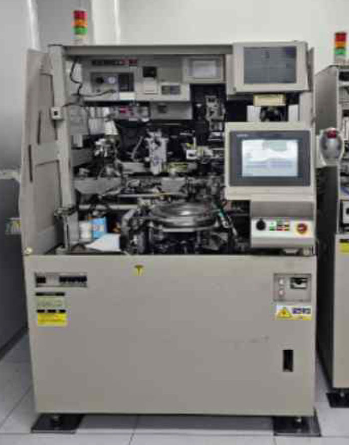
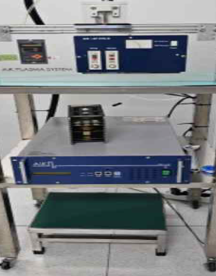
Post-process packaging training ability
반도체 후공정 패키징 교육 시설
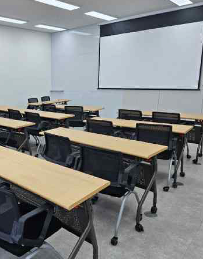
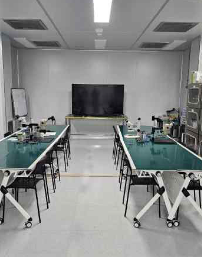
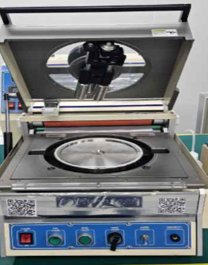
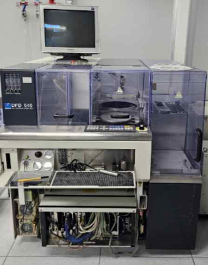
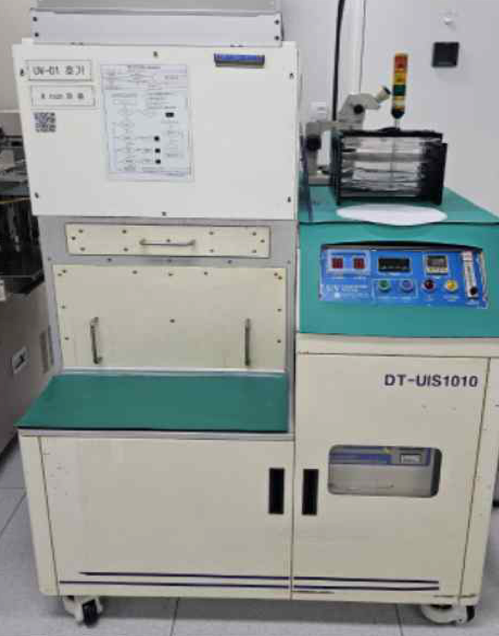
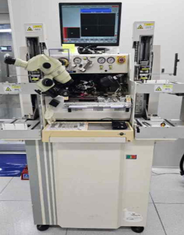
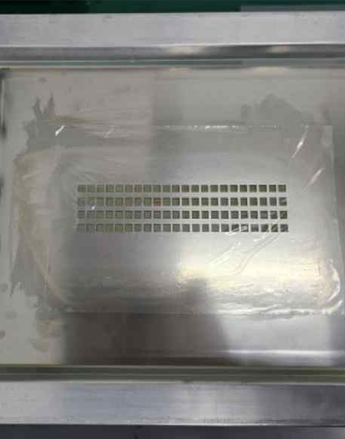
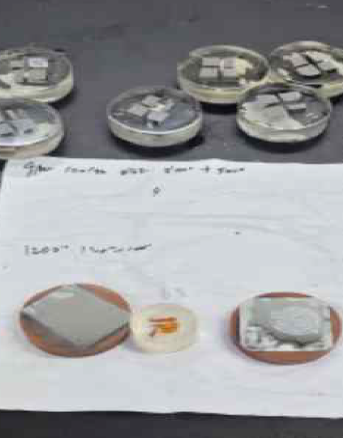
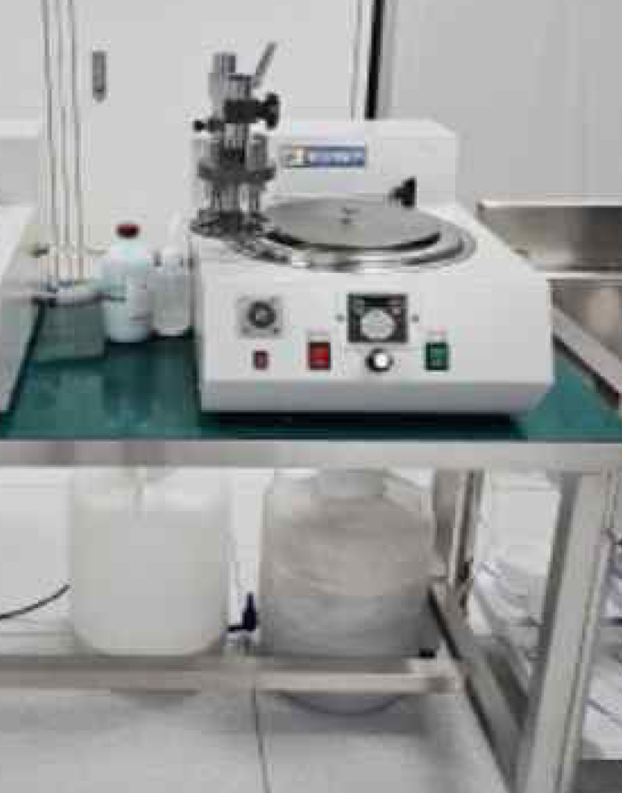
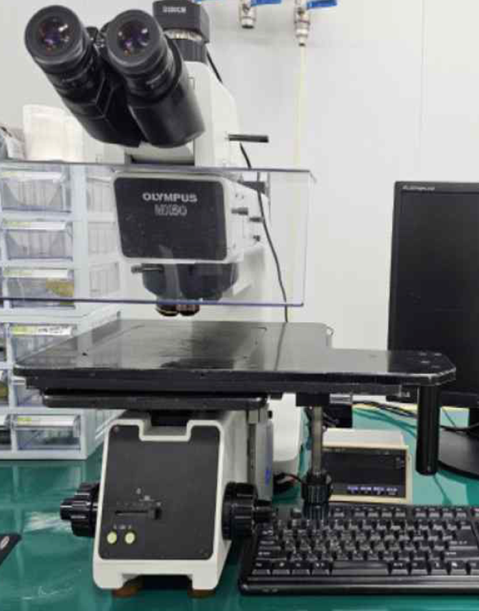
반도체 패키징 교육 장소 및 실습 장비
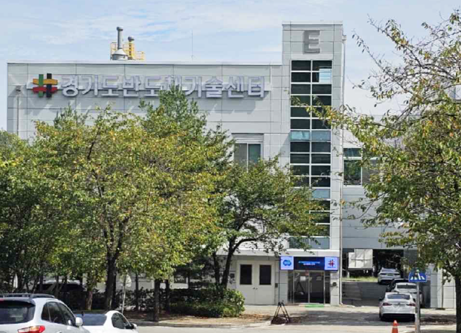
교육장소 : 경기도 차세대융합기술연구원 소재 (경기도 반도체 기술센타)
주 소 : 경기도 수원시 영통구 광교로 145(이의동 차세대융합기술연구원)
E동 E112호