About SPTS Future plans
핵심 공정에 대해 설비투자를 통한 반도체 인력육성양성 인프라 고도화 추진.
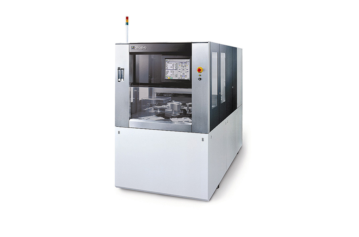
DGP8540 Back Grinder
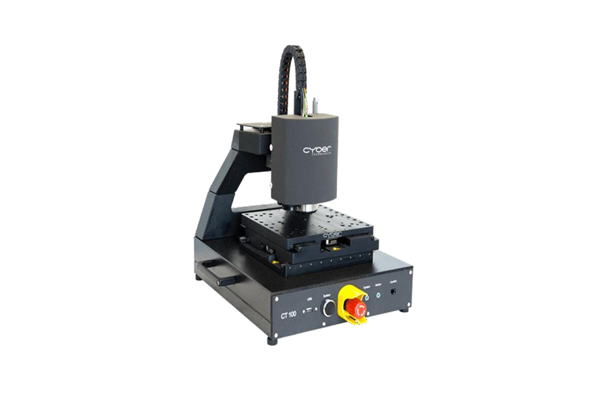
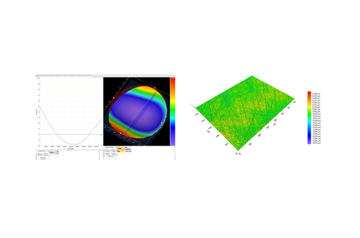
3D Measurement
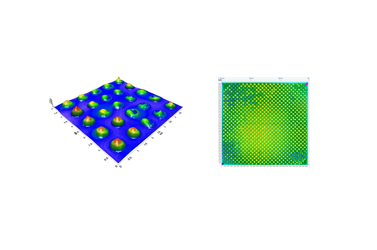
Bump Height pitch
-. Tape Mount
-. Wafer Dicing
-. UV System
-. Back Grind(Plan)
-. Tape Remover(Plan)
-. Material Properties
-. Capper Pillar Bonding
-. Au Bump Bonding
-. Under-fill Test
-. Flux Print
-. Ultrasonic Cleaning
-. Oven Bake
-. Molding
-. Cross Section
-. X-Ray (Plan)
-. SAIT (Plan)
-. 3D Measurement (Plan)
-. Wire Set-up
-. Wire Bonding
-. Wire Stud bump
-. Plasma system
-. FCBGA